Most Claude demos are software. This one is a circuit board.
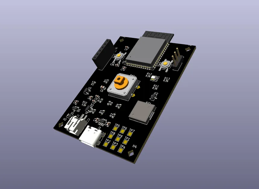
Open Telegraph is a pocket-size Morse key: an ESP32-S3, one button, one RGB LED, and a small battery. Plug it in over USB-C or pair it over Bluetooth and it types Morse into any device as a normal keyboard. It's fully open, down to the copper.
What we're trying to do
The Morse key is a starting point. Chouhan Industries is building toward consumer hardware you actually own: fully open, customizable down to the source files, and yours to build yourself, adapt to your needs, or simply buy finished. The thing that has always made open hardware slow is the design itself, holding a whole board's worth of constraints in your head and keeping every document honest. That's the part Claude changes.
We build it with Claude Code open on the repo, editing the real files:
- The KiCad schematic, one sheet per subsystem: USB input, charger and load-sharing, the 3.3 V rail, the ESP32-S3 with its reset and boot circuit, the key, jack, LED and sidetone, battery and USB sensing, and the headers
- The 2-layer PCB layout: 40 by 40 mm, 0.2 mm track and space, a full antenna keepout, and a bottom-layer ground pour
- Five design docs that have to stay in sync: the specification, the bill of materials with orderable part numbers, the ESP32-S3 pin assignment, the per-subsystem schematic values, and the placement and routing plan
- ERC on the schematic and DRC on the board, run through
kicad-cli
The one number the whole board is built around
There is no power switch. "Off" is the ESP32-S3 in deep sleep, and the whole board has to live inside about 25 µA while it's there. That single number decides most of the parts on the board.
| Mode | Draw | Endurance (250 mAh cell) |
|---|---|---|
| Deep sleep ("off") | ~25 µA | ~14 months |
| Bluetooth connected, keying | ~25 mA avg | ~10 hours |
| Charge from empty | 100 mA | ~3 hours |
Fourteen months of standby from a battery smaller than a stick of gum only works if nothing leaks. So a resistor that would draw 33 µA is not a rounding error, it's a bug. That framing is what makes the next few decisions non-obvious.
Why it's actually useful
The hard part of hardware isn't drawing one circuit. It's keeping everything consistent when a decision changes, and picking parts that satisfy every constraint at once, not just the obvious one. A few real examples from this board.
No power switch
A real switch gives a true zero-draw "off," but it's a moving part, a hole in the enclosure, and another gesture on a one-button device. We talked it through and dropped it: "off" is just deep sleep, held on the key. The price is the ~25 µA budget above, and at that draw a 250 mAh cell still idles for over a year.
The regulator
The 3.3 V rail has to hold across a 3.0 to 4.75 V input, source a few hundred mA on radio bursts, and draw under ~8 µA asleep. That last one kills most parts: cheap LDOs sit at 60 to 100 µA quiescent, tripling the sleep budget on their own. We use the Torex XC6220B331 (~8 µA, 1.6 to 6.0 V in), with the reason written next to it so nobody swaps in something cheaper.
A resistor that must not exist
A straight key's mono plug grounds the jack's ring the whole time it's in, so a normal pullup on the dah pin (KEY_DAH, GPIO7) would leak ~33 µA forever and blow the 25 µA budget. So it gets no external pullup: firmware uses the ESP32-S3's internal one and releases it before sleep. Picking the part meant proving a resistor shouldn't be there, because a missing pullup looks like a mistake.
Reuse over new parts
Both jack lines need ESD protection, the key cable is an antenna next to a live radio. Instead of a new part, we reused the same USBLC6-2SC6 already on the USB lines (U4 becomes U5), its VBUS pin tied to 3.3 V so its diodes stay reverse-biased and add nothing to the sleep budget. One fewer BOM line.
The strapping-pin trap
The key is deliberately off GPIO0, a boot-strapping pin: sitting there, holding the key during a reset would drop the board into the ROM bootloader. It's on GPIO4 instead, RTC-capable, so it still wakes from deep sleep, and GPIO0 stays clean. Catching this means reading the module's strapping table before assigning a pin.
Placement that respects physics
No copper anywhere near the module's antenna, full keepout on any layer, out past the board edge. The ESD arrays sit right at the connectors they protect, because a clamp at the far end of a trace protects nothing. The button is dead center, because the button is the product.
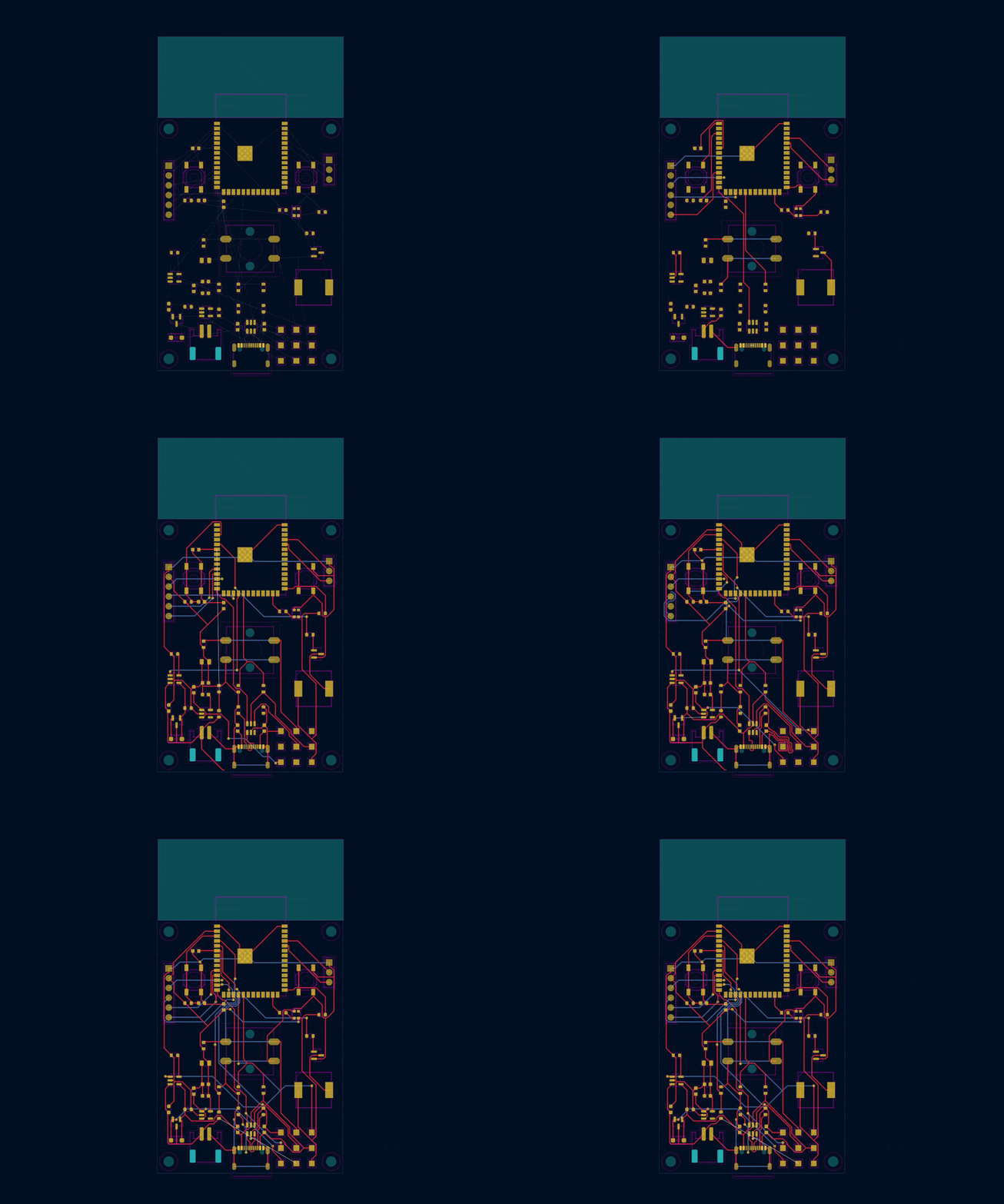
None of this is autocomplete. It's reading datasheets, holding a handful of constraints in your head at once, and writing down the reasoning so the next change doesn't quietly undo it.
How the workflow works
It's a loop, and it looks a lot like pair-programming, except the codebase is a circuit board.
- Start from the docs. Every decision lives in one of five markdown files, so Claude reads those first and knows the whole design, not just the part in front of it.
- Talk through the change. We describe what we want ("add an external key jack", "cut the sleep current"). Claude proposes the parts and circuit, and we push back until the reasoning holds up.
- Edit the real files. Claude writes the changes straight into the KiCad schematic and the design docs, using the same part names and net names everywhere so nothing drifts.
- Propagate. Change one value, like the charge current or a pin, and Claude carries it across every doc and the schematic that references it. This is the boring, easy-to-get-wrong step it's best at.
- Check the work. Claude reads the errors back and fixes them. Nothing is "done" until the tools agree.
- Write down why. Every real decision gets a one-line reason next to it, so the next change doesn't quietly undo it.
The check in step five is two commands, run the same way every time. Claude runs them, reads the report, and fixes what they flag:
# validate the schematic (parses the full sheet hierarchy)
kicad-cli sch erc --exit-code-violations -o erc.rpt \
  hardware/open-telegraph.kicad_sch

# validate the board against the design rules
kicad-cli pcb drc --exit-code-violations -o drc.rpt \
  hardware/open-telegraph.kicad_pcb
Then repeat. The docs are the memory, the KiCad files are the output, and the kicad-cli checks
are the safety net.
What this looks like live
Claude Code open on the real repo. Say "cut the sleep current" or "move the key off GPIO0" and watch it
propagate the change across all five docs and the schematic, keeping every net name and part number in
sync, then run kicad-cli ERC and DRC and read the violations back. A circuit board,
redesigned in front of you, in one prompt.
Where Claude fits
Not as an autorouter, and not as the engineer of record. As the reasoning layer over the whole design at once:
- Consistency. Change one value and it propagates across every doc, the BOM, and the schematic. No drift.
- Part choice. Hold every constraint at once, input range, current, quiescent draw, package, sourceable, not just the obvious one.
- Traps. Catch the datasheet rules, strapping pins, ADC limits, leaking pullups, before they ship.
- Rationale. Write the one-line why next to each decision, so the next change doesn't undo it.
The bench work, metering rails, routing copper, bring-up, stays human.
The point
The Morse key is just the proof. The product is the workflow: Claude as a co-designer that holds the constraints, picks the parts, lays out the board, and checks its own work, so one person can take a real product from idea to manufacturable files in days, not months. That's the thing worth shipping, a faster way to design and make hardware, and the board is just what it made first. It's all public (CERN-OHL-S v2.0), so anyone can run the same loop.